
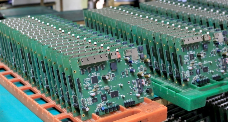
A Printed Circuit Board or PCB is an electronic component connecting different components together. Designing a PCB board is a complicated process that needs a lot of accuracy and precision. There are a few mistakes that may occur during the design process and they can affect the overall functionality of the board. Here are the common mistakes that may occur during PCB design process.
Incompetent Layout Techniques
PCB designers need to layout complex designs to design faster and smaller devices. There is an increasing demand for circuits that feature minimal footprints and designers have to utilize smaller components to reduce the footprint. These components are usually placed close together and there is a danger of the connections going wrong or not as desired, especially if you select an incompetent layout technique. When working with smaller pitches and higher pin counts, it is crucial to choose the right board layout technique for your PCB manufacturing process.
Improper Copper Thickness
For most designs one ounce of copper is usually selected as a finished thickness. One ounce of copper repeatedly fails to confirm enough plating in the holes. To make sure the PCB assembly and design is successful, you should be specific regarding the requirement parameters. To guarantee a successful design, it is essential to choose copper that has a finished thickness of about 1 to 2 ounces per square feet.
Incorrectly Placed Decoupling Capacitors
Decoupling capacitors are components that help in maintaining a stable voltage. These capacitors are usually placed on the power supply rail. For these capacitors to be effective, they should be placed extremely close to the pin that needs stable voltage. If these capacitors are placed incorrectly or far from the pin that needs stable voltage, then the capacitors will not work. This is a common mistake that most PCB assembly designers can detect before mass production of printed circuit boards.
No design Reviews
During the PCB assembly process, design review is a crucial process. Design reviews incorporate reviewing the design features, interconnection of circuits, and functioning of the assembled PCBs. When design reviews are performed, they can help in avoiding the most common PCB manufacturing mistakes that go unnoticed during the design process.
Lack Data of Backups
To guarantee perfect results during the PCB assembly process, different data and software are used. There are programs can help designers to develop complex PCB manufacturing designs. These programs have high speed and flexibility and as a result, the data can easily be lost before you have an opportunity to save them. To avoid all these issues and losing your designs, you must ensure that you save your data frequently. It is recommended to develop save points so that you if one storage area is corrupted, you will have saved and secured information that you can retrieve.
No communication
Productivity during PCB manufacturing processes can be brought about by stress, multitasking, and fatigue. These issues usually result in miscommunication that can increase the operation costs and time. To avoid all these problems, proper communication is necessary as it will give designers adequate time needed for designing PCBs. This can also ensure that the promised delivery date is achieved.
These are some of the common mistakes that can occur during the PCB design process. Ensure that you check these points above to avoid these mistakes. When you avoid these problems, they will enable you have a successful PCB manufacturing process. Furthermore, you can avoid the chances of ending up with ineffective and expensive prototypes that will take longer to get to the market.